
Energy Materials
Renewable energy harvesting and efficient energy utilization are essential for creating a sustainable future. In the WSI, we develop new semiconductors, catalytic assemblies, and nanosystems that are the engines of energy conversion devices, including solar fuels generators, photovoltaics, and solid state lighting. Advanced microscopic and spectroscopic characterization methods provide mechanistic insights that guide new strategies for fabrication of functional systems offering improved stabilities and efficiencies.
Project Modules

Integrated Photonics
One of our current research directions is to develop high-performance integrated photonic, quantum photonic and optoelectronic devices based on on-chip monolithically integrated quantum nanowire (NW) heterostructures. Specific examples include NW-based lasers and non-classical single photon emitters based on NW-QD (-quantum dot) devices for next-generation information technology, quantum communication and sensing. Hereby, an important task is to explore the optical and photonic responses of the respective systems using advanced confocal luminescence spectroscopy along with simulations, where e.g. the effects of the quantized electronic structure, light-matter interactions, or the coupling of light to on-chip photonic circuits are probed. The following key publications illustrate our current work on integrated photonic NW-based devices and their properties.
Discovery and development of advanced thin film semiconductors
Thin film semiconductors based on nitrides, oxynitrides, and oxides serve as versatile platforms for tailoring electronic and optical properties of materials. By leveraging advanced deposition techniques, such as reactive sputter deposition, molecular beam epitaxy, and solution-based processing, we explore novel material compositions with precisely controlled structures. A key focus of our research is the comprehensive characterization of these materials, including their elemental composition and atomic bonding environments, electronic structures, and excited state characteristics using a combination of lab- and synchrotron-based techniques. With this suite of complementary experimental tools, we investigate defects, doping strategies, and charge transport dynamics to understand and tune optical and electronic properties. These insights are crucial for controlling the functional properties of these materials for applications that include photoelectrochemical energy conversion, solar cells, and sustainable electronic devices.
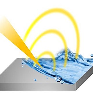
In situ & operando spectroscopy at reactive interfaces
To unlock the full potential of functional materials, it is essential to study their properties under realistic operating conditions. Our research focuses on the development of in situ and operando spectroscopic techniques that provide real-time insights into the structural, electronic, and chemical dynamics of thin films, electrocatalysts, and semiconductor systems. In particular, we employ near-ambient pressure X-ray photoelectron spectroscopy (NAP-XPS) to probe surface chemistry in reactive environments, transient absorption spectroscopy (TAS) to track charge carrier and electrochemical dynamics, Fourier-transform infrared (FTIR) spectroscopy to monitor molecular vibrations and reaction intermediates, and Raman spectroscopy to analyze structural transformations of materials driven away from equilibrium. These techniques allow us to correlate key energy conversion performance metrics with the electronic structure, defect states, and reaction mechanisms in dynamic environments. Our approach bridges fundamental materials science with innovative energy conversion concepts, enabling the design of more efficient and stable energy materials.
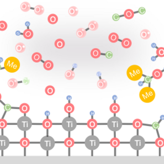
Tailored (photo)electrochemical interfaces
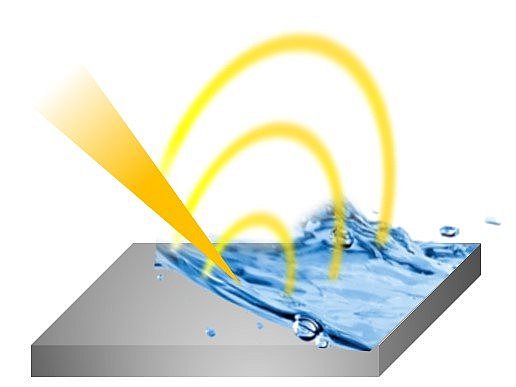
The performance of advanced energy materials is critically determined by their interfaces. In (photo)electrochemical systems, efficient charge transfer relies on the precise design of both solid-solid and solid-liquid interfaces. Our research focuses on tailoring these interfaces at the atomic- and nanoscale to precisely guide efficient energy conversion processes. A key aspect of this research is based on the alignment of energy levels at heterojunctions, which governs selective charge injection and extraction. In addition, we investigate semiconductor-liquid junctions, where interfacial electric fields and surface states play a crucial role in dictating reaction kinetics. Beyond material properties, we study how microenvironments around electrocatalysts – including local pH, ion distribution, and solvation effects – can influence reaction selectivity. These insights are applied to the development of materials for sustainable generation of chemicals from sunlight, with tailored interfacial properties enabling accelerated charge transfer, enhanced reaction selectivity, and improved conversion efficiency.
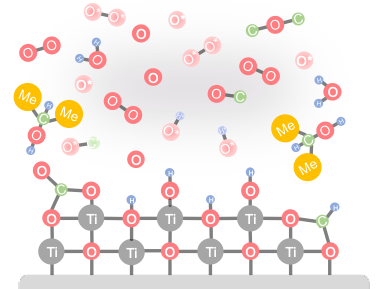
Ultrathin functional materials via atomic layer deposition
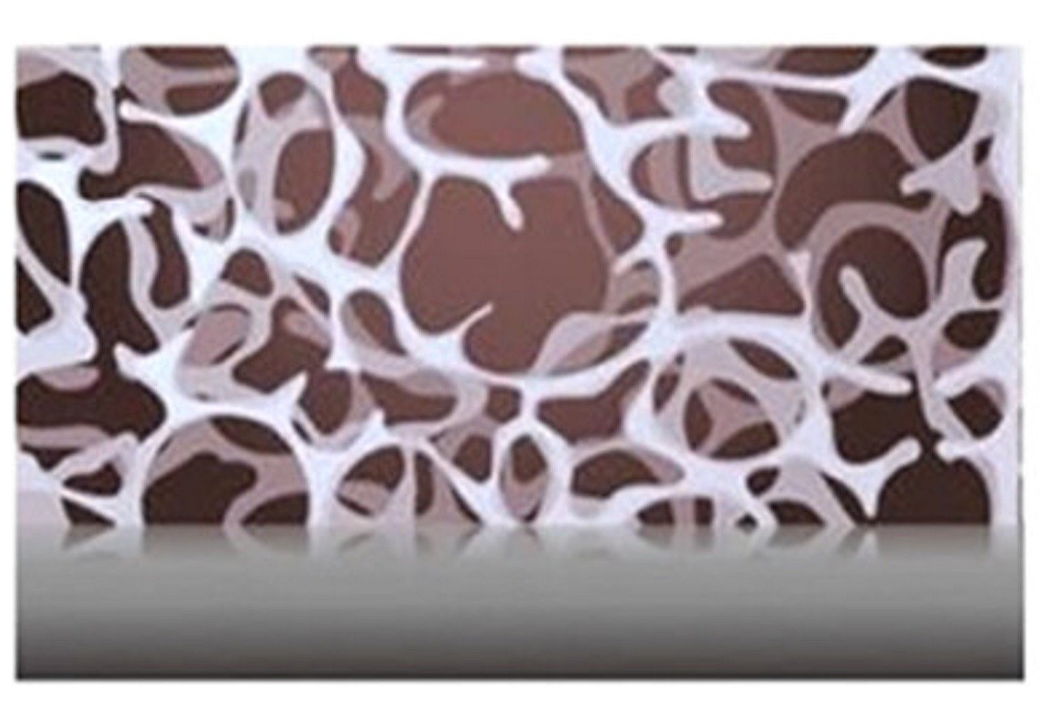
From tunable dielectrics integrated into nanoscale electronic devices to multifunctional coatings that promote efficient solar-to-chemical energy conversion, we make extensive use of atomic layer deposition (ALD) to precisely engineer interfaces, design novel heterostructures, and introduce defined functionalities at surfaces. Within this research, we develop novel ALD processes and materials, guided by in situ spectroscopic ellipsometry and mass spectrometry that offer real-time insights into nucleation dynamics, growth kinetics, defect formation, and film properties. Moving beyond traditional approaches, we explore advanced ALD strategies by, for example, integrating plasma-surface interactions to tune interfacial chemical and electronic properties, introducing external stimuli to achieve area-selective growth, and tailoring reaction conditions to shape nanoscale morphologies. By advancing ALD-based methods for precise interface and material control, our work contributes to the development of next-generation electronic, energy, and catalytic systems in which nanoscale structure-property relationships are critical.
Project Module
Integrated Photonics
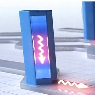
One of our current research directions is to develop high-performance integrated photonic, quantum photonic and optoelectronic devices based on on-chip monolithically integrated quantum nanowire (NW) heterostructures. Specific examples include NW-based lasers and non-classical single photon emitters based on NW-QD (-quantum dot) devices for next-generation information technology, quantum communication and sensing. Hereby, an important task is to explore the optical and photonic responses of the respective systems using advanced confocal luminescence spectroscopy along with simulations, where e.g. the effects of the quantized electronic structure, light-matter interactions, or the coupling of light to on-chip photonic circuits are probed. The following key publications illustrate our current work on integrated photonic NW-based devices and their properties.
Personnel
B. Alparslan, C. Doganlar, B. Haubmann, N. Isaev, H. W. Jeong, S. Meder, T. Schreitmüller, S. Werner, J. Zöllner
Publications
Project Module
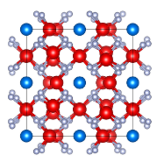
Discovery and development of advanced thin film semiconductors
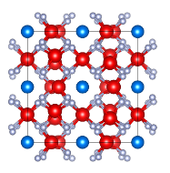
Thin film semiconductors based on nitrides, oxynitrides, and oxides serve as versatile platforms for tailoring electronic and optical properties of materials. By leveraging advanced deposition techniques, such as reactive sputter deposition, molecular beam epitaxy, and solution-based processing, we explore novel material compositions with precisely controlled structures. A key focus of our research is the comprehensive characterization of these materials, including their elemental composition and atomic bonding environments, electronic structures, and excited state characteristics using a combination of lab- and synchrotron-based techniques. With this suite of complementary experimental tools, we investigate defects, doping strategies, and charge transport dynamics to understand and tune optical and electronic properties. These insights are crucial for controlling the functional properties of these materials for applications that include photoelectrochemical energy conversion, solar cells, and sustainable electronic devices.
Project Module
In situ & operando spectroscopy at reactive interfaces
To unlock the full potential of functional materials, it is essential to study their properties under realistic operating conditions. Our research focuses on the development of in situ and operando spectroscopic techniques that provide real-time insights into the structural, electronic, and chemical dynamics of thin films, electrocatalysts, and semiconductor systems. In particular, we employ near-ambient pressure X-ray photoelectron spectroscopy (NAP-XPS) to probe surface chemistry in reactive environments, transient absorption spectroscopy (TAS) to track charge carrier and electrochemical dynamics, Fourier-transform infrared (FTIR) spectroscopy to monitor molecular vibrations and reaction intermediates, and Raman spectroscopy to analyze structural transformations of materials driven away from equilibrium. These techniques allow us to correlate key energy conversion performance metrics with the electronic structure, defect states, and reaction mechanisms in dynamic environments. Our approach bridges fundamental materials science with innovative energy conversion concepts, enabling the design of more efficient and stable energy materials.
Project Module
Tailored (photo)electrochemical interfaces
The performance of advanced energy materials is critically determined by their interfaces. In (photo)electrochemical systems, efficient charge transfer relies on the precise design of both solid-solid and solid-liquid interfaces. Our research focuses on tailoring these interfaces at the atomic- and nanoscale to precisely guide efficient energy conversion processes. A key aspect of this research is based on the alignment of energy levels at heterojunctions, which governs selective charge injection and extraction. In addition, we investigate semiconductor-liquid junctions, where interfacial electric fields and surface states play a crucial role in dictating reaction kinetics. Beyond material properties, we study how microenvironments around electrocatalysts – including local pH, ion distribution, and solvation effects – can influence reaction selectivity. These insights are applied to the development of materials for sustainable generation of chemicals from sunlight, with tailored interfacial properties enabling accelerated charge transfer, enhanced reaction selectivity, and improved conversion efficiency.
Project Module
Ultrathin functional materials via atomic layer deposition
From tunable dielectrics integrated into nanoscale electronic devices to multifunctional coatings that promote efficient solar-to-chemical energy conversion, we make extensive use of atomic layer deposition (ALD) to precisely engineer interfaces, design novel heterostructures, and introduce defined functionalities at surfaces. Within this research, we develop novel ALD processes and materials, guided by in situ spectroscopic ellipsometry and mass spectrometry that offer real-time insights into nucleation dynamics, growth kinetics, defect formation, and film properties. Moving beyond traditional approaches, we explore advanced ALD strategies by, for example, integrating plasma-surface interactions to tune interfacial chemical and electronic properties, introducing external stimuli to achieve area-selective growth, and tailoring reaction conditions to shape nanoscale morphologies. By advancing ALD-based methods for precise interface and material control, our work contributes to the development of next-generation electronic, energy, and catalytic systems in which nanoscale structure-property relationships are critical.