About the WSI

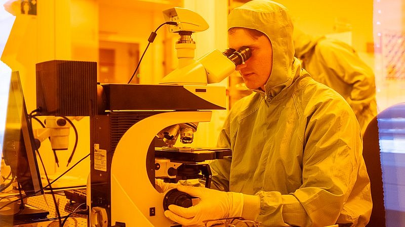
Today, the WSI and WSI Center for Nanotechnology and Nanomaterials (WSI-ZNN) buildings house laboratories and offices with a total floorspace of about 4500 m². At the heart of each of the two buildings are clean room facilities providing a total of ~450 m² for state-of-the-art semiconductor growth, nanofabrication and in-situ analytical technologies. Shared large scale facilities are housed within these laboratories for nanofabrication using focused Ga and He ions as well as state of the art electron beam lithography and MBE facilities for the growth of ultrapure materials. Looking back to the foundation of the institute, the building costs for the original WSI building (16.4 million DM) were initially covered by the Siemens company. TUM purchased the institute in 1992 as a central institute of the Technical University of Munich. The Bavarian State gave generous funding for the initial equipment (15 million DM) and created three new full professorships, with a total of 23 staff positions, one chair belonging to the department of electrical engineering and information sciences and two to the physics department. Due to serious space pressures within the original WSI building, WSI-ZNN was opened in 2010 to provide additional office and laboratory space, together with state-of-the-art infrastructure for nano-structuring, nano-spectroscopy and nano-analytics. 

The Institute

The following research groups have been established in the laboratories of WSI and WSI-ZNN:

  • Semiconductor Technology: Günter Weimann (from 1988 to 1995), Markus-Christian Amann (from 1997 - 2018), Mikhail Belkin (since 2019)
  • Experimental Semiconductor Physics I: Gerhard Abstreiter (1987 – 2013 and now TUM Emeritus of Excellence)
  • Semiconductor Nanostructures and Quantum Systems: Jonathan Finley (since 2013)
  • Hybrid Nanosystems – Nanoscale Optoelectronics : Alex Holleitner (since 2008)
  • Experimental Semiconductor Physics II : Erich Gornik (from 1988 to 1993), Martin Stutzmann (since 1993)
  • Theoretical Semiconductor Physics (Peter Vogl (1990-2016))
  • Experimental Semiconductor Physics - Energy Materials : Ian Sharp (since 2017)

The main research interests over the years have been:

  • Fabrication and characterization of new semiconductor materials, material combinations, as well as functionalization of surfaces
  • Development of novel methods for fabrication and characterization of nanostructures
  • Basic physics with emphasis on electronic and optical properties of low dimensional systems
  • Realisation of new semiconductor devices for applications in ultrafast electronics, optoelectronics, and as biological / chemical sensors
  • Theory and simulation of modern semiconductor materials and devices


The early projects concentrated on Si, GaAs, and InP based systems, with emphasis on heteroepitaxy with atomic scale precision.

Device oriented projects have been the development of ultrafast and low-noise III-V hetero-field-effect-transistors, laser diodes in the wavelength range from 980 nm to 2.7µm, vertical emitting laser diodes and Si / SiGe based devices. Fundamental research projects involved optical studies of quantum wires and dots, especially spatially resolved spectroscopy, transport and resonant tunneling in low dimensional systems, as well as the realization of novel devices based on quantum-effects. More recently, interest have shifted also towards emergent materials such as GaN and related alloys, diamond, group-III antimonides and 2D materials like graphene, topological insulators and transition metal dichalcogenides. Current research themes have a strong focus on Nanoscale Materials Science, Novel Spectroscopic and Analytical Methods, Quantum Information Science and Technology and Energy Sciences.


Text

text