
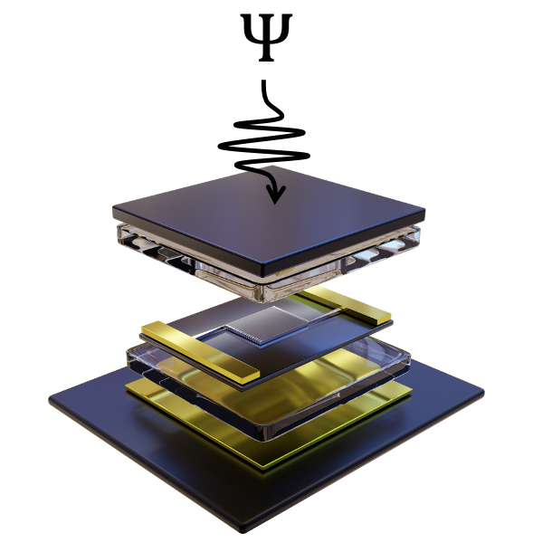
Quantum Technologies
Today, we are witnessing a scientific and technological revolution in which information science and quantum mechanics have been united into the common field of Quantum Information Science and Technology. We work on building next generation quantum devices and materials and explore their applications ranging from inherently secure communication and processing of information, to ultrasensitive sensors and transducers for precision metrology.
Project Modules
2D Magnetic Semiconductors
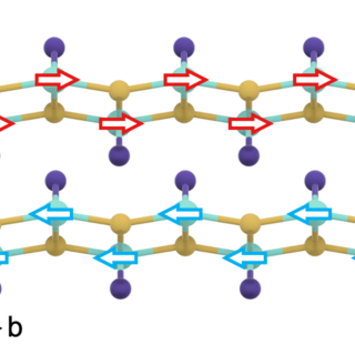
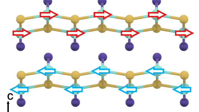
The chromium chalcogen halides (CrXH) are an emerging family of 2D semiconductors with a direct bandgap, highly anisotropic structural and electronic properties, and robust magnetic order with ordering temperatures up to room temperature. We seek to understand and engineer interactions between the magnetic order in CrXH compounds and the excitons they host. The unique magnetic and optical properties of CrXH materials present unique opportunities to develop spintronic devices with magnetic and optical controllability.

Synthetic superlattices and quantum simulation
Superlattices are artificial, periodic potentials which are used to confined particles and quasiparticles such as atoms, electrons, or excitons. If the trapped quasiparticles are allowed to interact, the resulting many-body state can capture essential behaviors of canonical quantum many-body theories (e.g. the Hubbard model). Such artificial quasiparticle lattices are often called analogue quantum simulators. A bit like a quantum wind tunnel, the quantum simulator serves as an engineerable scale model of a real physical system (electrons or other particles in a real crystalline solid) which allows us to probe complicated many-body physics with a high level of control. Such many-body physics are often hard to describe or predict theoretically, so our quantum simulators provide a route to benchmark leading theories and discover new phases of matter beyond current theoretical predictions.

Superconducting Nanowire Single Photon Detectors (SNSPDs)
Superconducting Nanowire Single-Photon Detectors (SNSPDs) are cutting-edge devices that enable the reliable detection of individual photons. They are formed by nano-patterning thin superconducting films to form nanowires wires. When operated at cryogenic temperatures, they deliver unmatched performance for quantum light detection with high efficiency, low noise, phonon-number resolution and picosecond photon timing precision. Thanks to their speed and sensitivity across a wide range of wavelengths spanning the visible to infrared, SNSPDs are a key technology for quantum communication, secure data transfer, advanced imaging, and fundamental scientific research. In the WSI we work closely with Munich Quantum Instruments GmbH and the QEC Group led by Kai Müller in the framework of several third-party research projects developing the materials technologies for SNSPDs made from polycrystalline superconducting thin films such as MoSi and NbTiN, as well as emergent van der Waals superconductors like NbSe2. We aim to understand the microscopic mechanisms governing the photo-detection process and apply e.g. local He-ion irradiation to enhance detector performance. Detectors are integrated into quantum photonic circuits with much scope for emergent quantum photonic technologies.
Nanoscale quantum magnetometry
The Nanoscale Quantum Magnetometer is a scanning probe microscope based on a single nitrogen vacancy (NV) center implanted in a diamond tip. The spin and optical dipole of the NV center can be used to measure stray electric and magnetic fields with nanoscale spatial resolution and exceptional dynamic range. The overarching goal of this instrument is to enable the study of nanoscale quantum materials and hybrid quantum systems using the high-resolution - and crucially - the multi-modal spectroscopy offered by tip-based NV quantum sensing. The unique proposed system moves the boundary of the experimental state-of-the-art by enabling tip-based, time resolved single spin spectroscopy at low temperatures in high magnetic fields. These capabilities are unique but necessary in order to manipulate and investigate the spin-and charge configurations of quantum matter. Moreover, the instrument has a sophisticated optical design to enable advanced optical spectroscopy experiments to correlate in real-time the nanoscale NV probe measurements with global observables. This project will enable completely new insight into the challenging but critical phase space from single particle interactions to a global quantum phase, and therefore overcomes the main experimental roadblocks to understand emergence in quantum matter.

Hexagonal Silicon Germanium
By far the most important chip materials are silicon (Si) and germanium (Ge), accounting for ~90% of global demand, and entirely dominating the electronics industry. Silicon chips could be much faster and more energy efficient if they operated with light. Silicon, germanium, and their alloys do not efficiently emit light in their naturally occurring, cubic, crystal form due to their indirect bandgap. However, a newly discovered allotrope of SiGe - hexagonal SiGe - efficiently emits light, holding much promise for silicon based classical and quantum photonic technologies.

Artificial Molecules as Spin-Photon Interfaces
III-V quantum dots (QDs) host ultrastable spin-qubits that can be optically addressed. They are used as deterministic and highly efficient sources of single photons, entangled photon pairs and streams of polarisation entangled photons for quantum photonic technologies. Single spins can create timed strings of entangled photons. Pairs of tunnel coupled spins in QD-molecules can be used to generate non-classical states of light with 2D entanglement structures needed for measurement based quantum information processing technologies.
Munich Initiative for Cross-Correlative Spin Microscopy (MICroCoSM)
The overarching goal of the Munich Initiative for Cross-Correlative Spin Microscopy (MICroCoSM) is to facilitate the study of nanoscale quantum materials and hybrid quantum systems using the high-resolution - and crucially - the multi-modal spectroscopy offered by tip-based nitrogen vacancy (NV) quantum sensing. The unique system installed in the labs of WSI moves the boundary of the experimental state-of-the-art by enabling tip-based, time resolved single spin spectroscopy at low temperatures in high magnetic fields. This is done using a low-temperature version of the ProteusQ scanning NV microscope from Qnami as a Spin-based Quantum Light Microscope (SQLM). It provides nanoscale access to magnetic properties of nano-materials subject to electrical / optical perturbations. Feel free to reach out to Prof. Finley if you are interested!
Quantum Transduction
A quantum transducer converts quantum information between different physical systems, such as photons, phonons, or spins. It enables communication across platforms that operate at distinct, and frequently disparate frequency or energy scales. Such devices are essential for linking quantum processors to long-distance quantum communication networks. Working as part of the Munich Quantum Valley project, WSI groups are working on the development of high bandwidth, semiconductor based quantum transducer modules capable of efficiently mapping between microwave quantum states of light and photons in the telecommunications band that can be distributed over optical fibers.

Neuromorphic Photonic Systems
Besides their spectacular optical, spin and electronic properties 2D materials can also exhibit ferroelectric order that arises as a consequence of the stacking order of van-der-Waals (vdW) layered materials and polarisation fields that emerge within the unit cell of the crystal. Such ferroelectricity can be controlled by strain & sliding of the component vdW layers of the materials. We explore high-quality 3R-stacked polytypes of TMDs that exhibit out-of-plane ferroelectricity. In 3R-TMD bilayers, sliding one monolayer a few Ångströms over the other flips the ferroelectric polarisation, a new ‘slidetronics’ concept in condensed matter physics inspired by twistronics. Such materials are deal for nanoscale systems in which ferroelectric order can be controlled with light, providing exciting new opportunities for optoelectronics, neuromorphic photonics, and sensing.
Van der Waals Materials for Integrated Nanophotonics
Integrated quantum photonics is pivotal for the implementation of quantum technologies and their transition from a laboratory to a real-life context. A photonic circuit may comprise one or more single photon sources and diverse components, such as waveguides, beam splitters, interferometers etc. required for steering and processing the quantum signals produced by the sources. In order to insure performance stability, as well as to minimise energy consumption, photonic circuits should integrate as many components as possible on a same chip. To this respect, a critical hurdle is represented by the necessity to assemble different materials that accomplish different tasks. In the VALERIA project our long term vision is to realise a single-material photonic platform exploiting the nano-structuring of transition metal dichalcogenides. The demonstration of this vision will be the fabrication of all-in-one devices made of a single TMD bulk crystal embedding site-controlled single photon emitters integrated with photonic crystal cavities and coupled to waveguides, beamsplitters amd non linear optical components.
Project Module
2D Magnetic Semiconductors
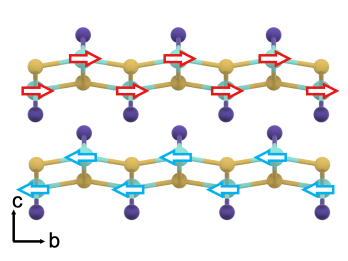
The chromium chalcogen halides (CrXH) are an emerging family of 2D semiconductors with a direct bandgap, highly anisotropic structural and electronic properties, and robust magnetic order with ordering temperatures up to room temperature. We seek to understand and engineer interactions between the magnetic order in CrXH compounds and the excitons they host. The unique magnetic and optical properties of CrXH materials present unique opportunities to develop spintronic devices with magnetic and optical controllability.
Lorem ipsum dolor sit amet, consectetur adipiscing elit. Morbi sapien mi, venenatis sed velit id, feugiat ultrices lectus. Pellentesque ornare felis sit amet est tristique, a pulvinar nunc finibus. Cras et libero sodales mi elementum tempus. Sed magna nisi, congue at rutrum nec, vulputate at neque. Quisque diam felis, bibendum eget velit et, efficitur euismod mauris. Suspendisse consectetur fermentum ligula sed lacinia. Donec imperdiet purus id rhoncus dictum. Duis et eleifend purus. Donec aliquet accumsan diam. Quisque euismod euismod nibh, sed tempor urna mattis vitae. In nec mi fermentum, sagittis libero sed, rutrum lorem.
Duis at sodales sapien. Donec nec justo dictum, vulputate tortor vitae, placerat dui. Pellentesque cursus ultricies mauris rutrum tristique. Nam sit amet leo ut dui tincidunt pretium eget quis sem. Morbi et nisi tellus. Vestibulum ullamcorper, elit ac sollicitudin blandit, risus risus egestas mauris, eu sagittis dolor lorem et ligula. Duis odio purus, rhoncus vitae nisl at, accumsan egestas sem. Aliquam erat volutpat. Morbi est ipsum, sollicitudin sit amet finibus at, sollicitudin ut purus. Duis varius eget quam a dictum. Cras in eleifend justo. Etiam vel aliquam odio.
Project Module
Synthetic superlattices and quantum simulation
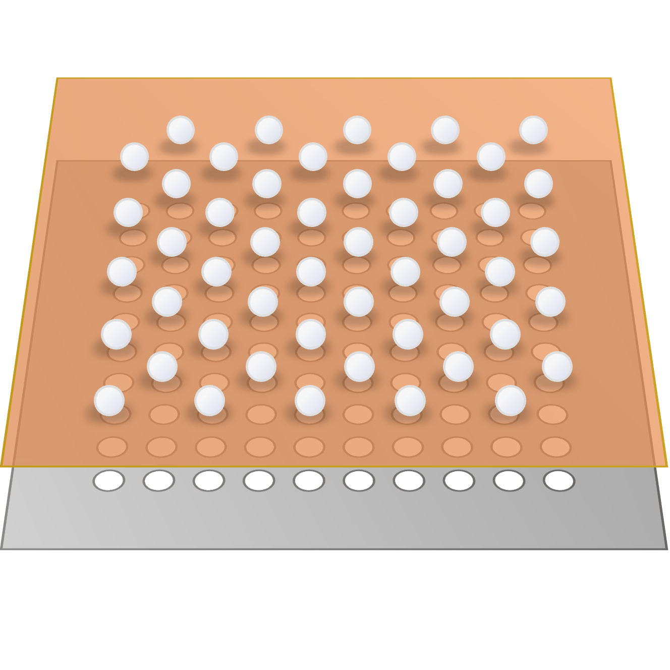
Superlattices are artificial, periodic potentials which are used to confined particles and quasiparticles such as atoms, electrons, or excitons. If the trapped quasiparticles are allowed to interact, the resulting many-body state can capture essential behaviors of canonical quantum many-body theories (e.g. the Hubbard model). Such artificial quasiparticle lattices are often called analogue quantum simulators. A bit like a quantum wind tunnel, the quantum simulator serves as an engineerable scale model of a real physical system (electrons or other particles in a real crystalline solid) which allows us to probe complicated many-body physics with a high level of control. Such many-body physics are often hard to describe or predict theoretically, so our quantum simulators provide a route to benchmark leading theories and discover new phases of matter beyond current theoretical predictions.
Our approach to quantum simulation is to create superlattices in 2D semiconductors by engineering an artificial electrostatic potential. This is accomplished by applying a bias voltage between a monolayer semiconductor and a nearby thin graphite layer which has been patterned with a periodic array of holes, generating a periodic potential/electric field profile in the 2D semiconductor layer which can trap charges. The depth of the superlattice potential can be easily tuned, and any lattice geometry can be implemented due to our top-down fabrication approach. We probe the superlattice devices using a combination of optical spectroscopy, relying on the natural sensitivity of the optically-active excitons to the correlated behavior of the charges in the superlattice, complemented by charge transport measurements.
Publications
Project Module
Superconducting Nanowire Single Photon Detectors (SNSPDs)
Superconducting Nanowire Single-Photon Detectors (SNSPDs) are cutting-edge devices that enable the reliable detection of individual photons. They are formed by nano-patterning thin superconducting films to form nanowires wires. When operated at cryogenic temperatures, they deliver unmatched performance for quantum light detection with high efficiency, low noise, phonon-number resolution and picosecond photon timing precision. Thanks to their speed and sensitivity across a wide range of wavelengths spanning the visible to infrared, SNSPDs are a key technology for quantum communication, secure data transfer, advanced imaging, and fundamental scientific research. In the WSI we work closely with Munich Quantum Instruments GmbH and the QEC Group led by Kai Müller in the framework of several third-party research projects developing the materials technologies for SNSPDs made from polycrystalline superconducting thin films such as MoSi and NbTiN, as well as emergent van der Waals superconductors like NbSe2. We aim to understand the microscopic mechanisms governing the photo-detection process and apply e.g. local He-ion irradiation to enhance detector performance. Detectors are integrated into quantum photonic circuits with much scope for emergent quantum photonic technologies.
Longer Text Description
Funding Agencies


Project Module
Nanoscale quantum magnetometry
The Nanoscale Quantum Magnetometer is a scanning probe microscope based on a single nitrogen vacancy (NV) center implanted in a diamond tip. The spin and optical dipole of the NV center can be used to measure stray electric and magnetic fields with nanoscale spatial resolution and exceptional dynamic range. The overarching goal of this instrument is to enable the study of nanoscale quantum materials and hybrid quantum systems using the high-resolution - and crucially - the multi-modal spectroscopy offered by tip-based NV quantum sensing. The unique proposed system moves the boundary of the experimental state-of-the-art by enabling tip-based, time resolved single spin spectroscopy at low temperatures in high magnetic fields. These capabilities are unique but necessary in order to manipulate and investigate the spin-and charge configurations of quantum matter. Moreover, the instrument has a sophisticated optical design to enable advanced optical spectroscopy experiments to correlate in real-time the nanoscale NV probe measurements with global observables. This project will enable completely new insight into the challenging but critical phase space from single particle interactions to a global quantum phase, and therefore overcomes the main experimental roadblocks to understand emergence in quantum matter.
A conventional approach to study many-body systems at the single-particle level would be with a series of specialized scanning tip microscopes, capable of probing many of the most fundamental properties of condensed matter systems, from sample morphology to magnetism, optical conductivity, electronic energy levels, etc. However, this approach requires different instruments or at least different probe tips, which practically often times bring along incompatible system or sample requirements. Crucially, however, the conventional approach is blind to the fact that emergent phases are intrinsically linked to all of the above – simultaneously - and most conventional methods can only probe static properties. Only an NV-based system is able to combine all sample properties to fully understand emergence in solids.
Project Module
Hexagonal Silicon Germanium

By far the most important chip materials are silicon (Si) and germanium (Ge), accounting for ~90% of global demand, and entirely dominating the electronics industry. Silicon chips could be much faster and more energy efficient if they operated with light. Silicon, germanium, and their alloys do not efficiently emit light in their naturally occurring, cubic, crystal form due to their indirect bandgap. However, a newly discovered allotrope of SiGe - hexagonal SiGe - efficiently emits light, holding much promise for silicon based classical and quantum photonic technologies.
Funding Agencies
Project Module
Artificial Molecules as Spin-Photon Interfaces

III-V quantum dots (QDs) host ultrastable spin-qubits that can be optically addressed. They are used as deterministic and highly efficient sources of single photons, entangled photon pairs and streams of polarisation entangled photons for quantum photonic technologies. Single spins can create timed strings of entangled photons. Pairs of tunnel coupled spins in QD-molecules can be used to generate non-classical states of light with 2D entanglement structures needed for measurement based quantum information processing technologies.
Funding Agencies

Project Module
Munich Initiative for Cross-Correlative Spin Microscopy (MICroCoSM)
The overarching goal of the Munich Initiative for Cross-Correlative Spin Microscopy (MICroCoSM) is to facilitate the study of nanoscale quantum materials and hybrid quantum systems using the high-resolution - and crucially - the multi-modal spectroscopy offered by tip-based nitrogen vacancy (NV) quantum sensing. The unique system installed in the labs of WSI moves the boundary of the experimental state-of-the-art by enabling tip-based, time resolved single spin spectroscopy at low temperatures in high magnetic fields. This is done using a low-temperature version of the ProteusQ scanning NV microscope from Qnami as a Spin-based Quantum Light Microscope (SQLM). It provides nanoscale access to magnetic properties of nano-materials subject to electrical / optical perturbations. Feel free to reach out to Prof. Finley if you are interested!
Funding Agencies
Project Module
Quantum Transduction
A quantum transducer converts quantum information between different physical systems, such as photons, phonons, or spins. It enables communication across platforms that operate at distinct, and frequently disparate frequency or energy scales. Such devices are essential for linking quantum processors to long-distance quantum communication networks. Working as part of the Munich Quantum Valley project, WSI groups are working on the development of high bandwidth, semiconductor based quantum transducer modules capable of efficiently mapping between microwave quantum states of light and photons in the telecommunications band that can be distributed over optical fibers.
Funding Agencies
Project Module
Neuromorphic Photonic Systems

Besides their spectacular optical, spin and electronic properties 2D materials can also exhibit ferroelectric order that arises as a consequence of the stacking order of van-der-Waals (vdW) layered materials and polarisation fields that emerge within the unit cell of the crystal. Such ferroelectricity can be controlled by strain & sliding of the component vdW layers of the materials. We explore high-quality 3R-stacked polytypes of TMDs that exhibit out-of-plane ferroelectricity. In 3R-TMD bilayers, sliding one monolayer a few Ångströms over the other flips the ferroelectric polarisation, a new ‘slidetronics’ concept in condensed matter physics inspired by twistronics. Such materials are deal for nanoscale systems in which ferroelectric order can be controlled with light, providing exciting new opportunities for optoelectronics, neuromorphic photonics, and sensing.
Project Module
Van der Waals Materials for Integrated Nanophotonics

Integrated quantum photonics is pivotal for the implementation of quantum technologies and their transition from a laboratory to a real-life context. A photonic circuit may comprise one or more single photon sources and diverse components, such as waveguides, beam splitters, interferometers etc. required for steering and processing the quantum signals produced by the sources. In order to insure performance stability, as well as to minimise energy consumption, photonic circuits should integrate as many components as possible on a same chip. To this respect, a critical hurdle is represented by the necessity to assemble different materials that accomplish different tasks. In the VALERIA project our long term vision is to realise a single-material photonic platform exploiting the nano-structuring of transition metal dichalcogenides. The demonstration of this vision will be the fabrication of all-in-one devices made of a single TMD bulk crystal embedding site-controlled single photon emitters integrated with photonic crystal cavities and coupled to waveguides, beamsplitters amd non linear optical components.
Funding Agencies