
Engineered Nanomaterials
Project Modules

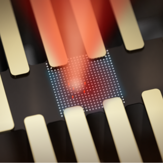
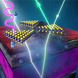
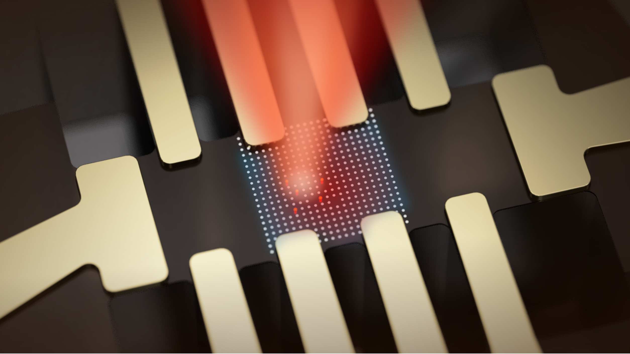
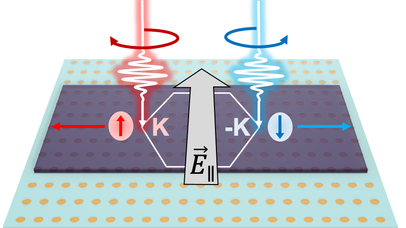
Synthetic superlattices and quantum simulation
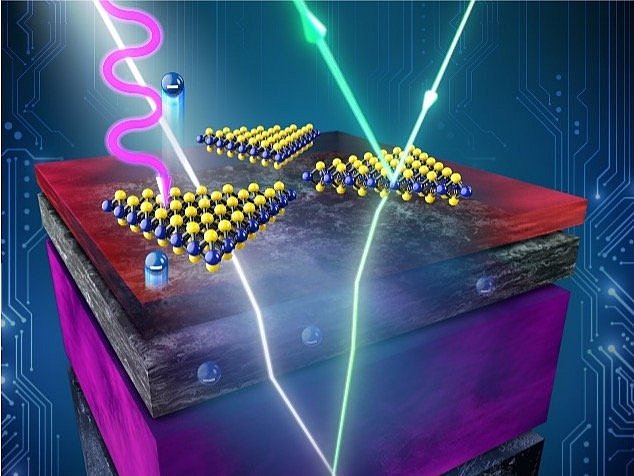
Superlattices are artificial, periodic potentials which are used to confined particles and quasiparticles such as atoms, electrons, or excitons. If the trapped quasiparticles are allowed to interact, the resulting many-body state can capture essential behaviors of canonical quantum many-body theories (e.g. the Hubbard model). Such artificial quasiparticle lattices are often called analogue quantum simulators. A bit like a quantum wind tunnel, the quantum simulator serves as an engineerable scale model of a real physical system (electrons or other particles in a real crystalline solid) which allows us to probe complicated many-body physics with a high level of control. Such many-body physics are often hard to describe or predict theoretically, so our quantum simulators provide a route to benchmark leading theories and discover new phases of matter beyond current theoretical predictions.
Test project module
Always visible
Discovery and development of advanced thin film semiconductors
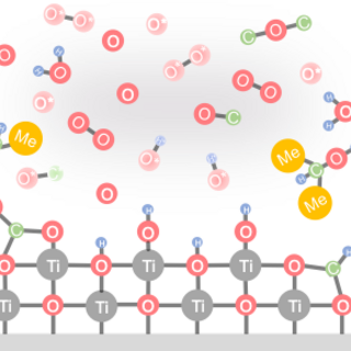
Thin film semiconductors based on nitrides, oxynitrides, and oxides serve as versatile platforms for tailoring electronic and optical properties of materials. By leveraging advanced deposition techniques, such as reactive sputter deposition, molecular beam epitaxy, and solution-based processing, we explore novel material compositions with precisely controlled structures. A key focus of our research is the comprehensive characterization of these materials, including their elemental composition and atomic bonding environments, electronic structures, and excited state characteristics using a combination of lab- and synchrotron-based techniques. With this suite of complementary experimental tools, we investigate defects, doping strategies, and charge transport dynamics to understand and tune optical and electronic properties. These insights are crucial for controlling the functional properties of these materials for applications that include photoelectrochemical energy conversion, solar cells, and sustainable electronic devices.
In situ & operando spectroscopy at reactive interfaces
To unlock the full potential of functional materials, it is essential to study their properties under realistic operating conditions. Our research focuses on the development of in situ and operando spectroscopic techniques that provide real-time insights into the structural, electronic, and chemical dynamics of thin films, electrocatalysts, and semiconductor systems. In particular, we employ near-ambient pressure X-ray photoelectron spectroscopy (NAP-XPS) to probe surface chemistry in reactive environments, transient absorption spectroscopy (TAS) to track charge carrier and electrochemical dynamics, Fourier-transform infrared (FTIR) spectroscopy to monitor molecular vibrations and reaction intermediates, and Raman spectroscopy to analyze structural transformations of materials driven away from equilibrium. These techniques allow us to correlate key energy conversion performance metrics with the electronic structure, defect states, and reaction mechanisms in dynamic environments. Our approach bridges fundamental materials science with innovative energy conversion concepts, enabling the design of more efficient and stable energy materials.
Tailored (photo)electrochemical interfaces
The performance of advanced energy materials is critically determined by their interfaces. In (photo)electrochemical systems, efficient charge transfer relies on the precise design of both solid-solid and solid-liquid interfaces. Our research focuses on tailoring these interfaces at the atomic- and nanoscale to precisely guide efficient energy conversion processes. A key aspect of this research is based on the alignment of energy levels at heterojunctions, which governs selective charge injection and extraction. In addition, we investigate semiconductor-liquid junctions, where interfacial electric fields and surface states play a crucial role in dictating reaction kinetics. Beyond material properties, we study how microenvironments around electrocatalysts – including local pH, ion distribution, and solvation effects – can influence reaction selectivity. These insights are applied to the development of materials for sustainable generation of chemicals from sunlight, with tailored interfacial properties enabling accelerated charge transfer, enhanced reaction selectivity, and improved conversion efficiency.
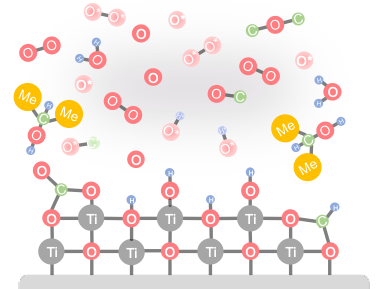
Ultrathin functional materials via atomic layer deposition
From tunable dielectrics integrated into nanoscale electronic devices to multifunctional coatings that promote efficient solar-to-chemical energy conversion, we make extensive use of atomic layer deposition (ALD) to precisely engineer interfaces, design novel heterostructures, and introduce defined functionalities at surfaces. Within this research, we develop novel ALD processes and materials, guided by in situ spectroscopic ellipsometry and mass spectrometry that offer real-time insights into nucleation dynamics, growth kinetics, defect formation, and film properties. Moving beyond traditional approaches, we explore advanced ALD strategies by, for example, integrating plasma-surface interactions to tune interfacial chemical and electronic properties, introducing external stimuli to achieve area-selective growth, and tailoring reaction conditions to shape nanoscale morphologies. By advancing ALD-based methods for precise interface and material control, our work contributes to the development of next-generation electronic, energy, and catalytic systems in which nanoscale structure-property relationships are critical.
2D Semiconductor Assemblies
While 2D semiconductors offer unique electronic and optical properties, realization of their full potential requires scalable growth and controlled integration into functional assemblies. In our research, we aim to create defined 2D/3D heterostructures using chemical vapor deposition (CVD) of transition metal dichalcogenides (TMDs) onto engineered substrates. These heterostructures include thin film junctions and laterally patterned substrates that enable precise spatial control of the 2D material and its electronic environment. In addition, we take advantage of low-temperature atomic layer deposition (ALD) processes to precisely tune interaction lengths and strengths between TMDs and their surroundings. A major emphasis of this work on 2D semiconductor assemblies is devoted to elucidating interfacial mechanisms that govern charge transfer pathways, energetic alignment, and structural and chemical interactions, providing a basis for future applications spanning from advanced optoelectronics to photocatalytic energy conversion.
Project Module
Synthetic superlattices and quantum simulation
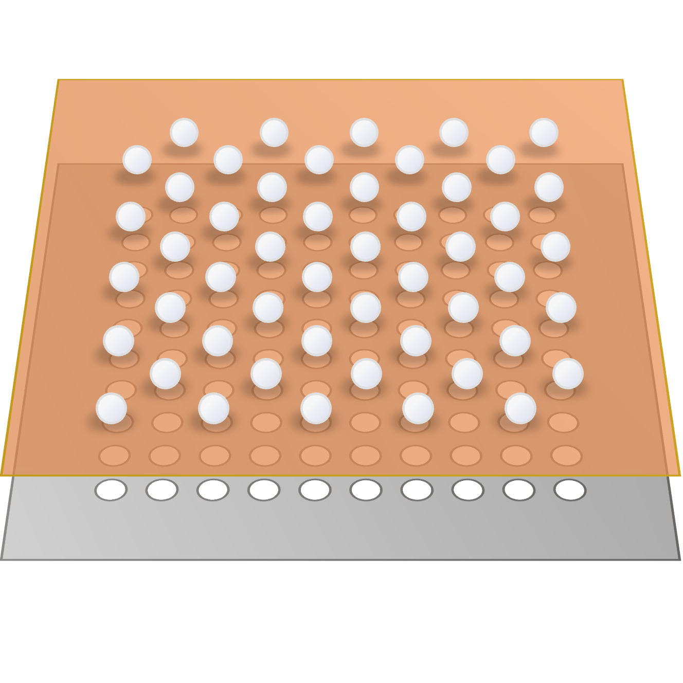
Superlattices are artificial, periodic potentials which are used to confined particles and quasiparticles such as atoms, electrons, or excitons. If the trapped quasiparticles are allowed to interact, the resulting many-body state can capture essential behaviors of canonical quantum many-body theories (e.g. the Hubbard model). Such artificial quasiparticle lattices are often called analogue quantum simulators. A bit like a quantum wind tunnel, the quantum simulator serves as an engineerable scale model of a real physical system (electrons or other particles in a real crystalline solid) which allows us to probe complicated many-body physics with a high level of control. Such many-body physics are often hard to describe or predict theoretically, so our quantum simulators provide a route to benchmark leading theories and discover new phases of matter beyond current theoretical predictions.
Our approach to quantum simulation is to create superlattices in 2D semiconductors by engineering an artificial electrostatic potential. This is accomplished by applying a bias voltage between a monolayer semiconductor and a nearby thin graphite layer which has been patterned with a periodic array of holes, generating a periodic potential/electric field profile in the 2D semiconductor layer which can trap charges. The depth of the superlattice potential can be easily tuned, and any lattice geometry can be implemented due to our top-down fabrication approach. We probe the superlattice devices using a combination of optical spectroscopy, relying on the natural sensitivity of the optically-active excitons to the correlated behavior of the charges in the superlattice, complemented by charge transport measurements.
Publications
Project Module
Test project module
Always visible
Above image
Publications
Project Module
Discovery and development of advanced thin film semiconductors
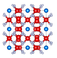
Thin film semiconductors based on nitrides, oxynitrides, and oxides serve as versatile platforms for tailoring electronic and optical properties of materials. By leveraging advanced deposition techniques, such as reactive sputter deposition, molecular beam epitaxy, and solution-based processing, we explore novel material compositions with precisely controlled structures. A key focus of our research is the comprehensive characterization of these materials, including their elemental composition and atomic bonding environments, electronic structures, and excited state characteristics using a combination of lab- and synchrotron-based techniques. With this suite of complementary experimental tools, we investigate defects, doping strategies, and charge transport dynamics to understand and tune optical and electronic properties. These insights are crucial for controlling the functional properties of these materials for applications that include photoelectrochemical energy conversion, solar cells, and sustainable electronic devices.
Project Module
In situ & operando spectroscopy at reactive interfaces
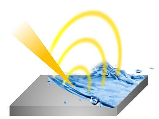
To unlock the full potential of functional materials, it is essential to study their properties under realistic operating conditions. Our research focuses on the development of in situ and operando spectroscopic techniques that provide real-time insights into the structural, electronic, and chemical dynamics of thin films, electrocatalysts, and semiconductor systems. In particular, we employ near-ambient pressure X-ray photoelectron spectroscopy (NAP-XPS) to probe surface chemistry in reactive environments, transient absorption spectroscopy (TAS) to track charge carrier and electrochemical dynamics, Fourier-transform infrared (FTIR) spectroscopy to monitor molecular vibrations and reaction intermediates, and Raman spectroscopy to analyze structural transformations of materials driven away from equilibrium. These techniques allow us to correlate key energy conversion performance metrics with the electronic structure, defect states, and reaction mechanisms in dynamic environments. Our approach bridges fundamental materials science with innovative energy conversion concepts, enabling the design of more efficient and stable energy materials.
Project Module
Tailored (photo)electrochemical interfaces
The performance of advanced energy materials is critically determined by their interfaces. In (photo)electrochemical systems, efficient charge transfer relies on the precise design of both solid-solid and solid-liquid interfaces. Our research focuses on tailoring these interfaces at the atomic- and nanoscale to precisely guide efficient energy conversion processes. A key aspect of this research is based on the alignment of energy levels at heterojunctions, which governs selective charge injection and extraction. In addition, we investigate semiconductor-liquid junctions, where interfacial electric fields and surface states play a crucial role in dictating reaction kinetics. Beyond material properties, we study how microenvironments around electrocatalysts – including local pH, ion distribution, and solvation effects – can influence reaction selectivity. These insights are applied to the development of materials for sustainable generation of chemicals from sunlight, with tailored interfacial properties enabling accelerated charge transfer, enhanced reaction selectivity, and improved conversion efficiency.
Project Module
Ultrathin functional materials via atomic layer deposition
From tunable dielectrics integrated into nanoscale electronic devices to multifunctional coatings that promote efficient solar-to-chemical energy conversion, we make extensive use of atomic layer deposition (ALD) to precisely engineer interfaces, design novel heterostructures, and introduce defined functionalities at surfaces. Within this research, we develop novel ALD processes and materials, guided by in situ spectroscopic ellipsometry and mass spectrometry that offer real-time insights into nucleation dynamics, growth kinetics, defect formation, and film properties. Moving beyond traditional approaches, we explore advanced ALD strategies by, for example, integrating plasma-surface interactions to tune interfacial chemical and electronic properties, introducing external stimuli to achieve area-selective growth, and tailoring reaction conditions to shape nanoscale morphologies. By advancing ALD-based methods for precise interface and material control, our work contributes to the development of next-generation electronic, energy, and catalytic systems in which nanoscale structure-property relationships are critical.
Project Module
2D Semiconductor Assemblies
While 2D semiconductors offer unique electronic and optical properties, realization of their full potential requires scalable growth and controlled integration into functional assemblies. In our research, we aim to create defined 2D/3D heterostructures using chemical vapor deposition (CVD) of transition metal dichalcogenides (TMDs) onto engineered substrates. These heterostructures include thin film junctions and laterally patterned substrates that enable precise spatial control of the 2D material and its electronic environment. In addition, we take advantage of low-temperature atomic layer deposition (ALD) processes to precisely tune interaction lengths and strengths between TMDs and their surroundings. A major emphasis of this work on 2D semiconductor assemblies is devoted to elucidating interfacial mechanisms that govern charge transfer pathways, energetic alignment, and structural and chemical interactions, providing a basis for future applications spanning from advanced optoelectronics to photocatalytic energy conversion.