
Nanofabrication
Nanofabrication is a cornerstone of modern semiconductor technology, enabling the creation of devices and structures at the nanometer scale. The research is crucial for the advancement of various technologies, including micro- and nanoelectronics, photonics, energy conversion and quantum computing.
Our research in nanofabrication focuses on the precise manipulation of materials at the atomic and molecular levels. By employing cutting-edge techniques such as electron and ion beam lithography as well as atomic layer deposition, we can create intricate patterns and structures with unprecedented accuracy even down to the single atom level. These techniques allow us to fabricate components that are smaller, faster, and more efficient than ever before.

We aim at structuring materials down to the atomic level or to dimensions specific to the envisioned experiment.
The Center for Nanotechnology and Nanomaterials
The Walter Schottky institute of the TUM operates the Center for Nanotechnologies and Nanomaterials (ZNN), as a shared nanofabrication facility. Students, researchers, and scholars from the greater scientific Munich area have access to state-of-the-art nanolithography and -analytic instruments for building and characterizing nanoscale electronic, optoelectronic, and photonic circuits. The nanofabrication methodologies include ebeam-, focused-ion-beam-, and helium-ion-lithography.
Project Modules

Synthetic superlattices and quantum simulation
Superlattices are artificial, periodic potentials which are used to confined particles and quasiparticles such as atoms, electrons, or excitons. If the trapped quasiparticles are allowed to interact, the resulting many-body state can capture essential behaviors of canonical quantum many-body theories (e.g. the Hubbard model). Such artificial quasiparticle lattices are often called analogue quantum simulators. A bit like a quantum wind tunnel, the quantum simulator serves as an engineerable scale model of a real physical system (electrons or other particles in a real crystalline solid) which allows us to probe complicated many-body physics with a high level of control. Such many-body physics are often hard to describe or predict theoretically, so our quantum simulators provide a route to benchmark leading theories and discover new phases of matter beyond current theoretical predictions.
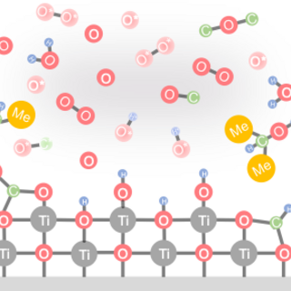
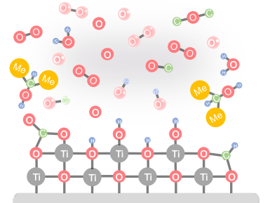
Ultrathin functional materials via atomic layer deposition
From tunable dielectrics integrated into nanoscale electronic devices to multifunctional coatings that promote efficient solar-to-chemical energy conversion, we make extensive use of atomic layer deposition (ALD) to precisely engineer interfaces, design novel heterostructures, and introduce defined functionalities at surfaces. Within this research, we develop novel ALD processes and materials, guided by in situ spectroscopic ellipsometry and mass spectrometry that offer real-time insights into nucleation dynamics, growth kinetics, defect formation, and film properties. Moving beyond traditional approaches, we explore advanced ALD strategies by, for example, integrating plasma-surface interactions to tune interfacial chemical and electronic properties, introducing external stimuli to achieve area-selective growth, and tailoring reaction conditions to shape nanoscale morphologies. By advancing ALD-based methods for precise interface and material control, our work contributes to the development of next-generation electronic, energy, and catalytic systems in which nanoscale structure-property relationships are critical.
2D Semiconductor Assemblies
While 2D semiconductors offer unique electronic and optical properties, realization of their full potential requires scalable growth and controlled integration into functional assemblies. In our research, we aim to create defined 2D/3D heterostructures using chemical vapor deposition (CVD) of transition metal dichalcogenides (TMDs) onto engineered substrates. These heterostructures include thin film junctions and laterally patterned substrates that enable precise spatial control of the 2D material and its electronic environment. In addition, we take advantage of low-temperature atomic layer deposition (ALD) processes to precisely tune interaction lengths and strengths between TMDs and their surroundings. A major emphasis of this work on 2D semiconductor assemblies is devoted to elucidating interfacial mechanisms that govern charge transfer pathways, energetic alignment, and structural and chemical interactions, providing a basis for future applications spanning from advanced optoelectronics to photocatalytic energy conversion.

Superconducting Nanowire Single Photon Detectors (SNSPDs)
Superconducting Nanowire Single-Photon Detectors (SNSPDs) are cutting-edge devices that enable the reliable detection of individual photons. They are formed by nano-patterning thin superconducting films to form nanowires wires. When operated at cryogenic temperatures, they deliver unmatched performance for quantum light detection with high efficiency, low noise, phonon-number resolution and picosecond photon timing precision. Thanks to their speed and sensitivity across a wide range of wavelengths spanning the visible to infrared, SNSPDs are a key technology for quantum communication, secure data transfer, advanced imaging, and fundamental scientific research. In the WSI we work closely with Munich Quantum Instruments GmbH and the QEC Group led by Kai Müller in the framework of several third-party research projects developing the materials technologies for SNSPDs made from polycrystalline superconducting thin films such as MoSi and NbTiN, as well as emergent van der Waals superconductors like NbSe2. We aim to understand the microscopic mechanisms governing the photo-detection process and apply e.g. local He-ion irradiation to enhance detector performance. Detectors are integrated into quantum photonic circuits with much scope for emergent quantum photonic technologies.
Hexagonal Silicon Germanium
By far the most important chip materials are silicon (Si) and germanium (Ge), accounting for ~90% of global demand, and entirely dominating the electronics industry. Silicon chips could be much faster and more energy efficient if they operated with light. Silicon, germanium, and their alloys do not efficiently emit light in their naturally occurring, cubic, crystal form due to their indirect bandgap. However, a newly discovered allotrope of SiGe - hexagonal SiGe - efficiently emits light, holding much promise for silicon based classical and quantum photonic technologies.

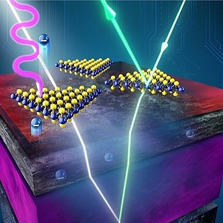
Neuromorphic Photonic Systems
Besides their spectacular optical, spin and electronic properties 2D materials can also exhibit ferroelectric order that arises as a consequence of the stacking order of van-der-Waals (vdW) layered materials and polarisation fields that emerge within the unit cell of the crystal. Such ferroelectricity can be controlled by strain & sliding of the component vdW layers of the materials. We explore high-quality 3R-stacked polytypes of TMDs that exhibit out-of-plane ferroelectricity. In 3R-TMD bilayers, sliding one monolayer a few Ångströms over the other flips the ferroelectric polarisation, a new ‘slidetronics’ concept in condensed matter physics inspired by twistronics. Such materials are deal for nanoscale systems in which ferroelectric order can be controlled with light, providing exciting new opportunities for optoelectronics, neuromorphic photonics, and sensing.
Project Module
Synthetic superlattices and quantum simulation
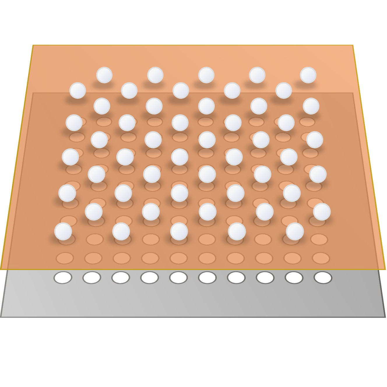
Superlattices are artificial, periodic potentials which are used to confined particles and quasiparticles such as atoms, electrons, or excitons. If the trapped quasiparticles are allowed to interact, the resulting many-body state can capture essential behaviors of canonical quantum many-body theories (e.g. the Hubbard model). Such artificial quasiparticle lattices are often called analogue quantum simulators. A bit like a quantum wind tunnel, the quantum simulator serves as an engineerable scale model of a real physical system (electrons or other particles in a real crystalline solid) which allows us to probe complicated many-body physics with a high level of control. Such many-body physics are often hard to describe or predict theoretically, so our quantum simulators provide a route to benchmark leading theories and discover new phases of matter beyond current theoretical predictions.
Our approach to quantum simulation is to create superlattices in 2D semiconductors by engineering an artificial electrostatic potential. This is accomplished by applying a bias voltage between a monolayer semiconductor and a nearby thin graphite layer which has been patterned with a periodic array of holes, generating a periodic potential/electric field profile in the 2D semiconductor layer which can trap charges. The depth of the superlattice potential can be easily tuned, and any lattice geometry can be implemented due to our top-down fabrication approach. We probe the superlattice devices using a combination of optical spectroscopy, relying on the natural sensitivity of the optically-active excitons to the correlated behavior of the charges in the superlattice, complemented by charge transport measurements.
Publications
Project Module
Ultrathin functional materials via atomic layer deposition
From tunable dielectrics integrated into nanoscale electronic devices to multifunctional coatings that promote efficient solar-to-chemical energy conversion, we make extensive use of atomic layer deposition (ALD) to precisely engineer interfaces, design novel heterostructures, and introduce defined functionalities at surfaces. Within this research, we develop novel ALD processes and materials, guided by in situ spectroscopic ellipsometry and mass spectrometry that offer real-time insights into nucleation dynamics, growth kinetics, defect formation, and film properties. Moving beyond traditional approaches, we explore advanced ALD strategies by, for example, integrating plasma-surface interactions to tune interfacial chemical and electronic properties, introducing external stimuli to achieve area-selective growth, and tailoring reaction conditions to shape nanoscale morphologies. By advancing ALD-based methods for precise interface and material control, our work contributes to the development of next-generation electronic, energy, and catalytic systems in which nanoscale structure-property relationships are critical.
Project Module
2D Semiconductor Assemblies
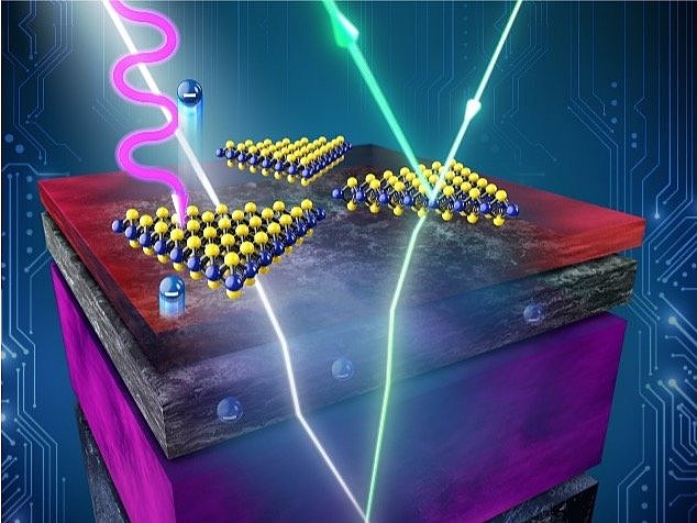
While 2D semiconductors offer unique electronic and optical properties, realization of their full potential requires scalable growth and controlled integration into functional assemblies. In our research, we aim to create defined 2D/3D heterostructures using chemical vapor deposition (CVD) of transition metal dichalcogenides (TMDs) onto engineered substrates. These heterostructures include thin film junctions and laterally patterned substrates that enable precise spatial control of the 2D material and its electronic environment. In addition, we take advantage of low-temperature atomic layer deposition (ALD) processes to precisely tune interaction lengths and strengths between TMDs and their surroundings. A major emphasis of this work on 2D semiconductor assemblies is devoted to elucidating interfacial mechanisms that govern charge transfer pathways, energetic alignment, and structural and chemical interactions, providing a basis for future applications spanning from advanced optoelectronics to photocatalytic energy conversion.
Project Module
Superconducting Nanowire Single Photon Detectors (SNSPDs)
Superconducting Nanowire Single-Photon Detectors (SNSPDs) are cutting-edge devices that enable the reliable detection of individual photons. They are formed by nano-patterning thin superconducting films to form nanowires wires. When operated at cryogenic temperatures, they deliver unmatched performance for quantum light detection with high efficiency, low noise, phonon-number resolution and picosecond photon timing precision. Thanks to their speed and sensitivity across a wide range of wavelengths spanning the visible to infrared, SNSPDs are a key technology for quantum communication, secure data transfer, advanced imaging, and fundamental scientific research. In the WSI we work closely with Munich Quantum Instruments GmbH and the QEC Group led by Kai Müller in the framework of several third-party research projects developing the materials technologies for SNSPDs made from polycrystalline superconducting thin films such as MoSi and NbTiN, as well as emergent van der Waals superconductors like NbSe2. We aim to understand the microscopic mechanisms governing the photo-detection process and apply e.g. local He-ion irradiation to enhance detector performance. Detectors are integrated into quantum photonic circuits with much scope for emergent quantum photonic technologies.
Longer Text Description
Funding Agencies


Project Module
Hexagonal Silicon Germanium

By far the most important chip materials are silicon (Si) and germanium (Ge), accounting for ~90% of global demand, and entirely dominating the electronics industry. Silicon chips could be much faster and more energy efficient if they operated with light. Silicon, germanium, and their alloys do not efficiently emit light in their naturally occurring, cubic, crystal form due to their indirect bandgap. However, a newly discovered allotrope of SiGe - hexagonal SiGe - efficiently emits light, holding much promise for silicon based classical and quantum photonic technologies.
Funding Agencies
Project Module
Neuromorphic Photonic Systems

Besides their spectacular optical, spin and electronic properties 2D materials can also exhibit ferroelectric order that arises as a consequence of the stacking order of van-der-Waals (vdW) layered materials and polarisation fields that emerge within the unit cell of the crystal. Such ferroelectricity can be controlled by strain & sliding of the component vdW layers of the materials. We explore high-quality 3R-stacked polytypes of TMDs that exhibit out-of-plane ferroelectricity. In 3R-TMD bilayers, sliding one monolayer a few Ångströms over the other flips the ferroelectric polarisation, a new ‘slidetronics’ concept in condensed matter physics inspired by twistronics. Such materials are deal for nanoscale systems in which ferroelectric order can be controlled with light, providing exciting new opportunities for optoelectronics, neuromorphic photonics, and sensing.